Representing crystal structures: descriptors
The first necessary step to perform any machine learning and/or automatized analysis on materials science data is to represent the material under consideration in a way that is understandable for a computer. This representation - termed descriptor - should contain all the relevant information on the system needed for the desired learning task.
Starting from crystal structure, provided as ASE (Atomistic Simulation Environment) Atoms object [link], the code allows to calculate different representations. Currently, the following descriptors (i.e. function to represent crystal structures) are implemented:
ai4materials.descriptors.atomic_featuresreturns the atomic features corresponding to the chemical species of the system [1]ai4materials.descriptors.diffraction2dcalculates the two-dimensional diffraction fingerprint [2]ai4materials.descriptors.diffraction3dcalculates the three-dimensional diffraction fingerprint [3]ai4materials.descriptors.prdfcalculates the partial radial distribution function [4]ai4materials.descriptors.SOAPcalculates the SOAP descriptor [5]
For example of descriptors’ usage and their references, see below.
Example: atomic features
It was recently shown in Ref. [1] that the crystal structure of binary compounds can be predicted using compressed-sensing technique using atomic features only.
The code below illustrates how to retrieve atomic features for one crystal structure. It performs the following steps:
- build a NaCl crystal structure using the ASE package
- calculate atomic features using the descriptor
ai4materials.descriptors.atomic_features.AtomicFeatures - retrieve the atomic features of this crystal structure as the panda dataframe
nacl_atomic_features - save this table to file.
import sys
import os.path

atomic_data_dir = os.path.abspath(os.path.normpath("/home/ziletti/nomad/nomad-lab-base/analysis-tools/atomic-data"))
sys.path.insert(0, atomic_data_dir)

from ase.spacegroup import crystal
from ai4materials.utils.utils_config import set_configs
from ai4materials.utils.utils_config import setup_logger
from ai4materials.descriptors.atomic_features import AtomicFeatures
from nomadcore.local_meta_info import loadJsonFile, InfoKindEl

# setup configs
configs = set_configs(main_folder='./desc_atom_features_ai4materials')
logger = setup_logger(configs, level='INFO', display_configs=False)

desc_file_name = 'atomic_features_try1'

# build atomic structure
structure = crystal(['Na', 'Cl'], [(0, 0, 0), (0.5, 0.5, 0.5)], spacegroup=225, cellpar=[5.64, 5.64, 5.64, 90, 90, 90])

selected_feature_list = ['atomic_ionization_potential', 'atomic_electron_affinity',
                         'atomic_rs_max', 'atomic_rp_max', 'atomic_rd_max']


# define and calculate descriptor
kwargs = {'feature_order_by': 'atomic_mulliken_electronegativity', 'energy_unit': 'eV', 'length_unit': 'angstrom'}

descriptor = AtomicFeatures(configs=configs, **kwargs)

structure_result = descriptor.calculate(structure, selected_feature_list=selected_feature_list)
nacl_atomic_features = structure_result.info['descriptor']['atomic_features_table']

# write table to file
nacl_atomic_features.to_csv('nacl_atomic_features_table.csv', float_format='%.4f')
This is the table (saved in the file nacl_atomic_features_table.csv) containing the atomic features obtained using the code above:
| ordered_chemical_symbols | atomic_ionization_potential(A) | atomic_electron_affinity(A) | atomic_rs_max(A) | atomic_rp_max(A) | atomic_rd_max(A) | atomic_ionization_potential(B) | atomic_electron_affinity(B) | atomic_rs_max(B) | atomic_rp_max(B) | atomic_rd_max(B) | |
|---|---|---|---|---|---|---|---|---|---|---|---|
| 0 | NaCl | -5.2231 | -0.7157 | 1.7100 | 2.6000 | 6.5700 | -13.9018 | -3.9708 | 0.6800 | 0.7600 | 1.6700 |
Example: two-dimensional diffraction fingerprint
The two-dimensional diffraction fingerprint was introduced in Ref. [2].
The code below illustrates how to calculate the two-dimensional diffraction fingerprint for a supercell of face-center-cubic aluminium containing approximately 256 atoms, performing following steps:
- build a face-centered-cubic aluminium crystal structure using the ASE package
- create a supercell using the function
ai4materials.utils.utils_crystals.create_supercell - calculate the two-dimensional diffraction fingerprint of this crystal structure as the numpy.array
intensity_rgb - convert the two-dimensional diffraction fingerprint as RGB image and write it to file.
from ase.spacegroup import crystal
from ase.io import write
from ai4materials.descriptors.diffraction2d import Diffraction2D
from ai4materials.utils.utils_config import set_configs
from ai4materials.utils.utils_crystals import create_supercell
import numpy as np
from PIL import Image

# setup configs
configs = set_configs(main_folder='./desc_2d_diff_ai4materials')

# create the fcc aluminium structure
fcc_al = crystal('Al', [(0, 0, 0)], spacegroup=225, cellpar=[4.05, 4.05, 4.05, 90, 90, 90])
structure = create_supercell(fcc_al, target_nb_atoms=256)

# calculate the two-dimensional diffraction fingerprint
descriptor = Diffraction2D(configs=configs)
structure_result = descriptor.calculate(structure)
intensity_rgb = structure_result.info['descriptor']['diffraction_2d_intensity']

# write the diffraction fingerprint as png image
rgb_array = np.zeros((intensity_rgb.shape[0], intensity_rgb.shape[1], intensity_rgb.shape[2]), 'uint8')
current_img = list(intensity_rgb.reshape(-1, intensity_rgb.shape[0], intensity_rgb.shape[1]))
for ix_ch in range(len(current_img)):
    rgb_array[..., ix_ch] = current_img[ix_ch] * 255
img = Image.fromarray(rgb_array)
img = img.resize([256, 256], Image.ANTIALIAS)
img.save('fcc_al_diffraction2d_fingerprint.png')
This is the calculated two-dimensional diffraction fingerprint for face-centered-cubic aluminium:
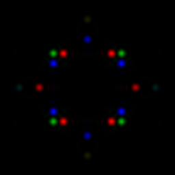
Implementation details of the two-dimensional diffraction fingerprint can be found at
ai4materials.descriptors.diffraction2d.
Example: three-dimensional diffraction fingerprint
The three-dimensional diffraction fingerprint was introduced in Ref. [3].
The code below illustrates how to calculate the three-dimensional diffraction fingerprint for a supercell of face-center-cubic aluminium containing approximately 256 atoms, performing following steps:
- build a face-centered-cubic aluminium crystal structure using the ASE package
- create a supercell using the function
ai4materials.utils.utils_crystals.create_supercell - calculate the three-dimensional diffraction fingerprint of this crystal structure as the numpy.array
diff3d_spectrum - convert the two-dimensional diffraction fingerprint as a heatmap image and write it to file.
from ase.spacegroup import crystal
import matplotlib.pyplot as plt
from ai4materials.descriptors.diffraction3d import DISH
from ai4materials.utils.utils_config import set_configs
from ai4materials.utils.utils_crystals import create_supercell
from scipy import ndimage

# setup configs
configs = set_configs(main_folder='./dish_ai4materials')

# create the fcc aluminium structure
fcc_al = crystal('Al', [(0, 0, 0)], spacegroup=225, cellpar=[4.05, 4.05, 4.05, 90, 90, 90])
structure = create_supercell(fcc_al, target_nb_atoms=256, random_rotation=True, cell_type='standard', optimal_supercell=False)

# calculate the two-dimensional diffraction fingerprint
descriptor = DISH(configs=configs)
structure_result = descriptor.calculate(structure)
diff3d_spectrum = descriptor.calculate(structure).info['descriptor']['diffraction_3d_sh_spectrum']

# plot the (enlarged) array as image (enlarging is unphysical, only for visualization purposes)
plt.imsave('fcc_al_diffraction3d_fingerprint.png', ndimage.zoom(diff3d_spectrum, (4, 4)))
This is the calculated three-dimensional diffraction fingerprint for face-centered-cubic aluminium (zoomed for visualization purposes):
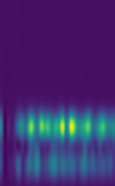
Implementation details of the three-dimensional diffraction fingerprint can be found at
ai4materials.descriptors.diffraction3d.
| [1] | (1, 2) L. M. Ghiringhelli, J. Vybiral, S. V. Levchenko, C. Draxl, and M. Scheffler, “Big Data of Materials Science: Critical Role of the Descriptor,” Physical Review Letters, vol. 114, no. 10, p. 105503 . [Link to article] |
| [2] | (1, 2) A. Ziletti, D. Kumar, M. Scheffler, and L. M. Ghiringhelli, “Insightful classification of crystal structures using deep learning,” Nature Communications, vol. 9, pp. 2775, 2018. [Link to article] |
| [3] | (1, 2)
|
| [4] | K. T. Schuett, H. Glawe, F. Brockherde, A. Sanna, K. R. M”uller, and E. K. U.Gross, “How to represent crystal structures for machine learning: Towards fast prediction of electronic properties,” Physical Review B, vol. 89, pp. 205118 (2014). [Link to article] |
| [5] | A. P. Bartók, R. Kondor, and G. Csányi, “On representing chemical environments,” Physical Review B, vol. 87, no. 18, p.184115 (2013) [Link to article] |
Section author: Angelo Ziletti <angelo.ziletti@gmail.com>
Submodules
- ai4materials.descriptors.atomic_features module
- ai4materials.descriptors.base_descriptor module
- ai4materials.descriptors.diffraction1d module
- ai4materials.descriptors.diffraction2d module
- ai4materials.descriptors.diffraction3d module
- ai4materials.descriptors.ft_soap_descriptor module
- ai4materials.descriptors.prdf module
- ai4materials.descriptors.quippy_soap_descriptor module
- ai4materials.descriptors.soap_model module